
Ultra-Clean CNC
Semiconductor Gas Distribution Plates
Ultra-clean CNC machined semiconductor gas distribution plates — electropolished internal channels Ra 0.4 µm, VCR/CF port interfaces, helium leak test <1×10⁻⁹ mbar·l/s, ISO Class 5 cleanroom packaging. For CVD, ALD, and etch process chambers.
mbar·l/s helium test
electropolished SUS316L
semiconductor grade
prototype orders
Semiconductor Gas Distribution Plate Challenges
Gas distribution plates for semiconductor process chambers require a combination of standards unmatched in any other CNC product: ultra-clean surfaces, sub-ppm particle generation, and helium-leak-tight interfaces.
Semiconductor Gas Distribution Plates We've Made
Real CNC machined projects — inspected and delivered.

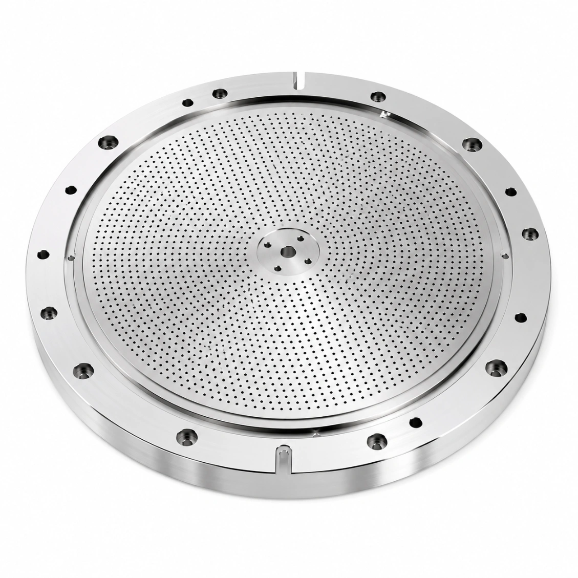


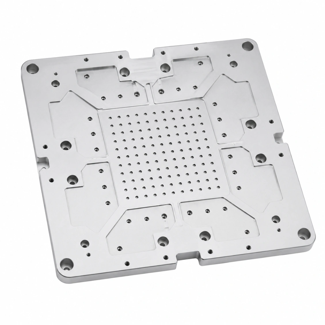


What We Can Deliver
Typical specifications for this product type. Confirm exact requirements at enquiry.
| Leak rate | <1×10⁻⁹ mbar·l/s (He) |
| Internal Ra | 0.4 µm (electropolished) |
| Orifice diameter tol. | ±0.005 mm |
| Port standards | VCR, CF, KF, custom face seal |
| Cleaning | IPA ultrasonic + N₂ dry + cleanroom pack |
| Particle generation | ISO Class 5 equivalent |
| Materials | SUS316L (std), Al 6061, Ti Grade 5 |
| Electropolish | Standard on all gas-wetted surfaces |
| Helium leak test | 100% every plate, certificate |
| Packaging | ISO Class 5 bag, double-sealed |
| Lead time (proto) | 8–12 days |
| Lead time (batch) | 14–20 days |
From Drawing to Finished Part
Upload your drawing — DFM review, machining, pressure/leak test if required, and shipping within agreed lead time.
Trusted by Engineers Worldwide
Frequently Asked Questions About Semiconductor Gas Distribution Plate Machining
Engineering and procurement questions answered by our team.