
CNC Machining Solutions forSemiconductor Equipment Components
Precision-machined components for vacuum systems, wafer handling equipment, fluid control modules, and clean-process assemblies.
We machine vacuum chamber parts, gas distribution plates, wafer handling fixtures, manifold blocks, and high-flatness mounting structures for semiconductor fabrication equipment — with controlled surface finishes, clean packaging, and full dimensional documentation.
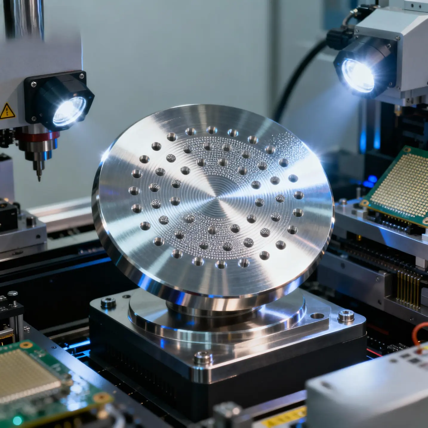
The manufacturing pain points our customers in this industry face most often — and how we address each one before it becomes a problem on your assembly line.

High Flatness and Precision Requirements
Wafer chuck interfaces, vacuum sealing flanges, and chamber bonding surfaces demand flatness within 0.01 mm and surface roughness Ra ≤ 0.4 μm. Standard milling is insufficient — we combine grinding and lapping to meet these requirements consistently.
Cleanliness-Sensitive Applications
Particles and surface contaminants in process chambers directly affect wafer yield. Parts must be machined, cleaned, and packaged in contamination-controlled conditions — we coordinate this as part of the standard delivery process.
Tight Dimensional Control for Equipment Interfaces
Gas showerhead hole arrays, manifold flow passage positions, and vacuum flange bolt circles must all meet tight positional tolerances for correct equipment assembly and sealing performance.
Stable Quality for High-Value Assemblies
Semiconductor equipment components are expensive to scrap and difficult to re-work after delivery. First-pass dimensional accuracy and consistent batch quality are not optional requirements — they are fundamental.
Precision components for vacuum chambers, process gas systems, wafer handling, and equipment structural assemblies. Every part is delivered clean-packaged with full dimensional documentation.
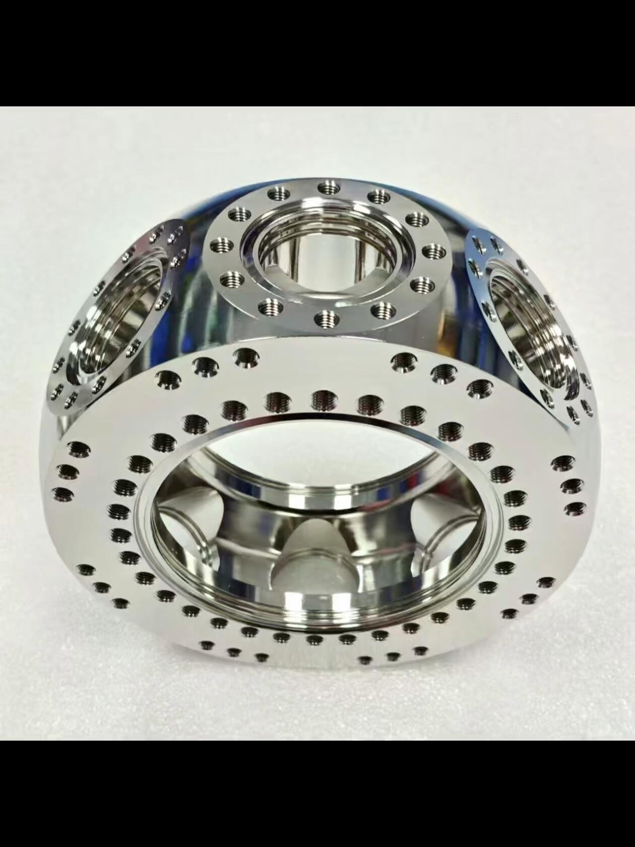

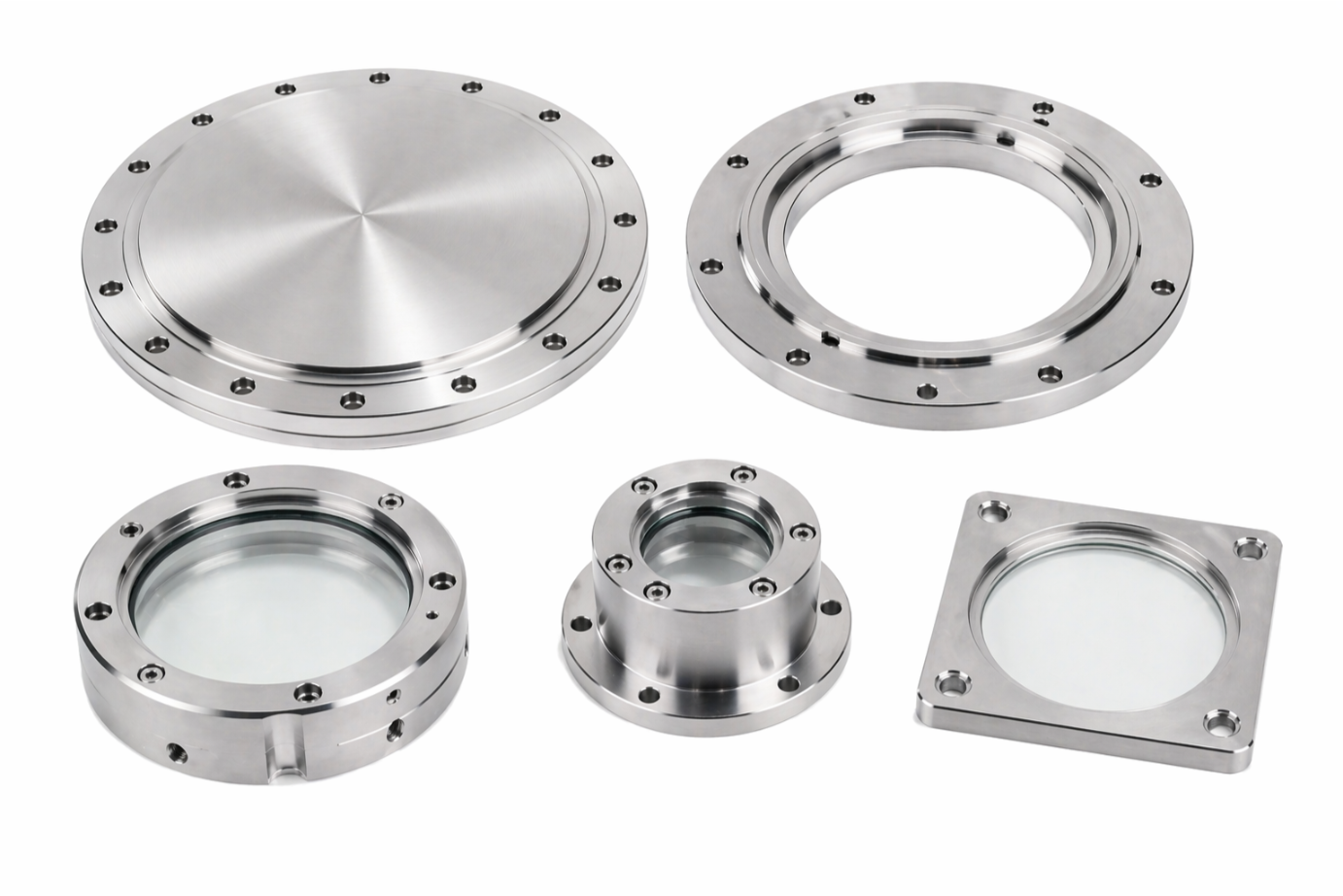
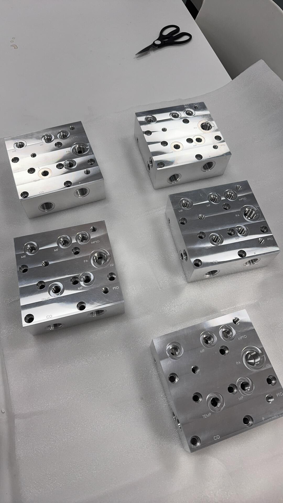
Specific machining, quality, and project support capabilities that match what this industry actually demands — not generic claims.


Surface Finish and Flatness Capability
We grind and lap critical sealing surfaces and wafer chuck interfaces to Ra ≤ 0.4 μm and flatness ≤ 0.01 mm — the levels required for vacuum sealing and wafer contact performance.
Clean Packaging as Standard
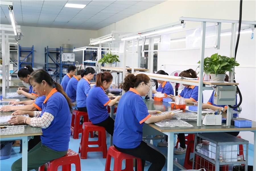
All semiconductor parts are ultrasonically cleaned, individually bagged in Class 100 polyethylene bags, and packaged in sealed containers with material certifications. No extra charge, no special request needed.
Full Dimensional Documentation
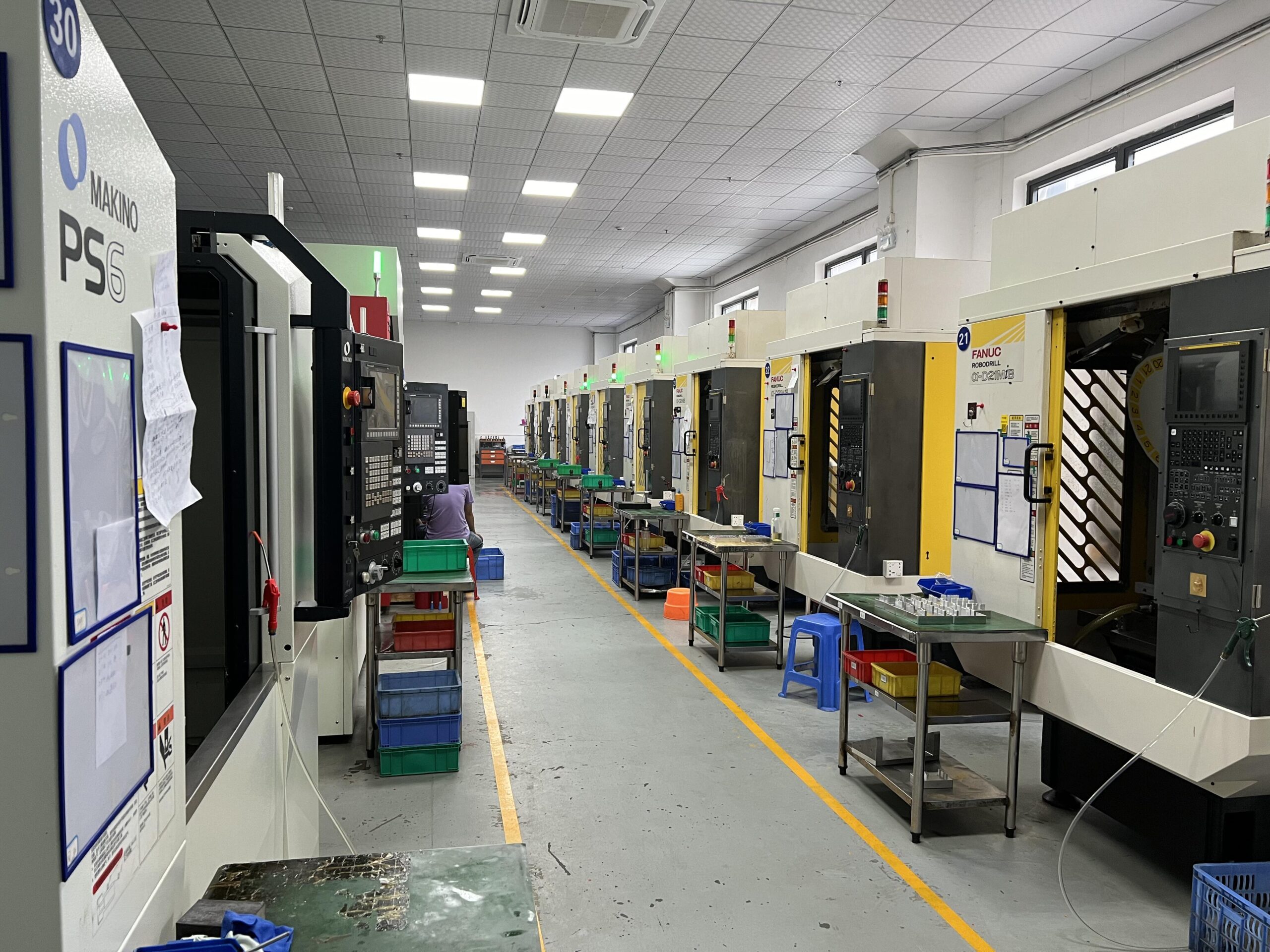
CMM first article reports with GD&T callouts — flatness, parallelism, true position, cylindricity — are issued as standard for all semiconductor equipment orders.
Stable Quality That Reduces Incoming Inspection Burden
Our documented inspection process means parts arrive with verified dimensions. Reduced receiving inspection, faster assembly start, fewer field failures from machining-related dimensional issues.
From your first drawing to stable production delivery — a clear process that keeps your development and production schedule on track.

Drawing Review & Material Confirmation
We review STEP files and 2D drawings, confirm material and cleanliness requirements, and flag any features requiring special process attention before quoting.
Quote with Complete Process Plan
You receive a quote that includes material, process sequence, surface finish, cleaning protocol, and packaging specification — not just a price.
First Article with Full CMM Report
First parts are machined, cleaned, and inspected. You receive a complete CMM dimensional report before bulk delivery begins.
Batch Delivery with Traceability
Production batches delivered with material certifications, process records, and CoC. Full lot traceability maintained for your supplier qualification records.
Material, machining process, and surface finish are coordinated at the quoting stage. Every combination below is validated on active customer programs.

A selection of completed projects from this industry. Every part was delivered with full CMM inspection report and material certification.
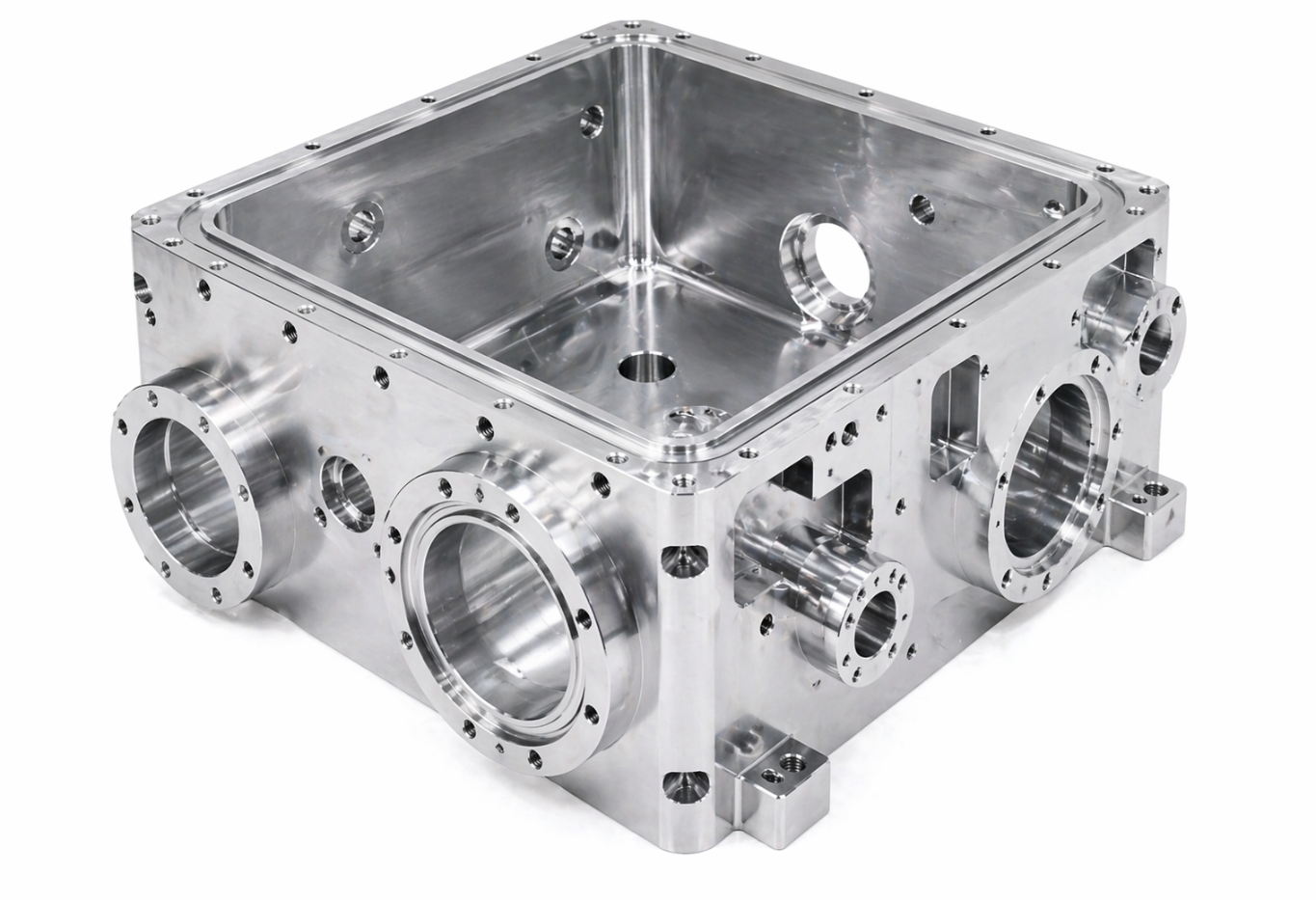
Aluminum Vacuum Chamber Body
6061-T6 Al vacuum chamber with anodized internal surfaces. Flatness ≤0.01 mm on sealing face, O-ring groove to AS568. Full CMM report, clean-packaged.

Gas Showerhead Distribution Plate
6061-T6 Al showerhead with 240 precision holes, ±0.01 mm position. 100% pin gauge inspection. Anodized and clean-packaged for CVD equipment OEM.
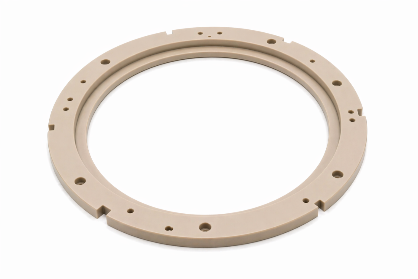
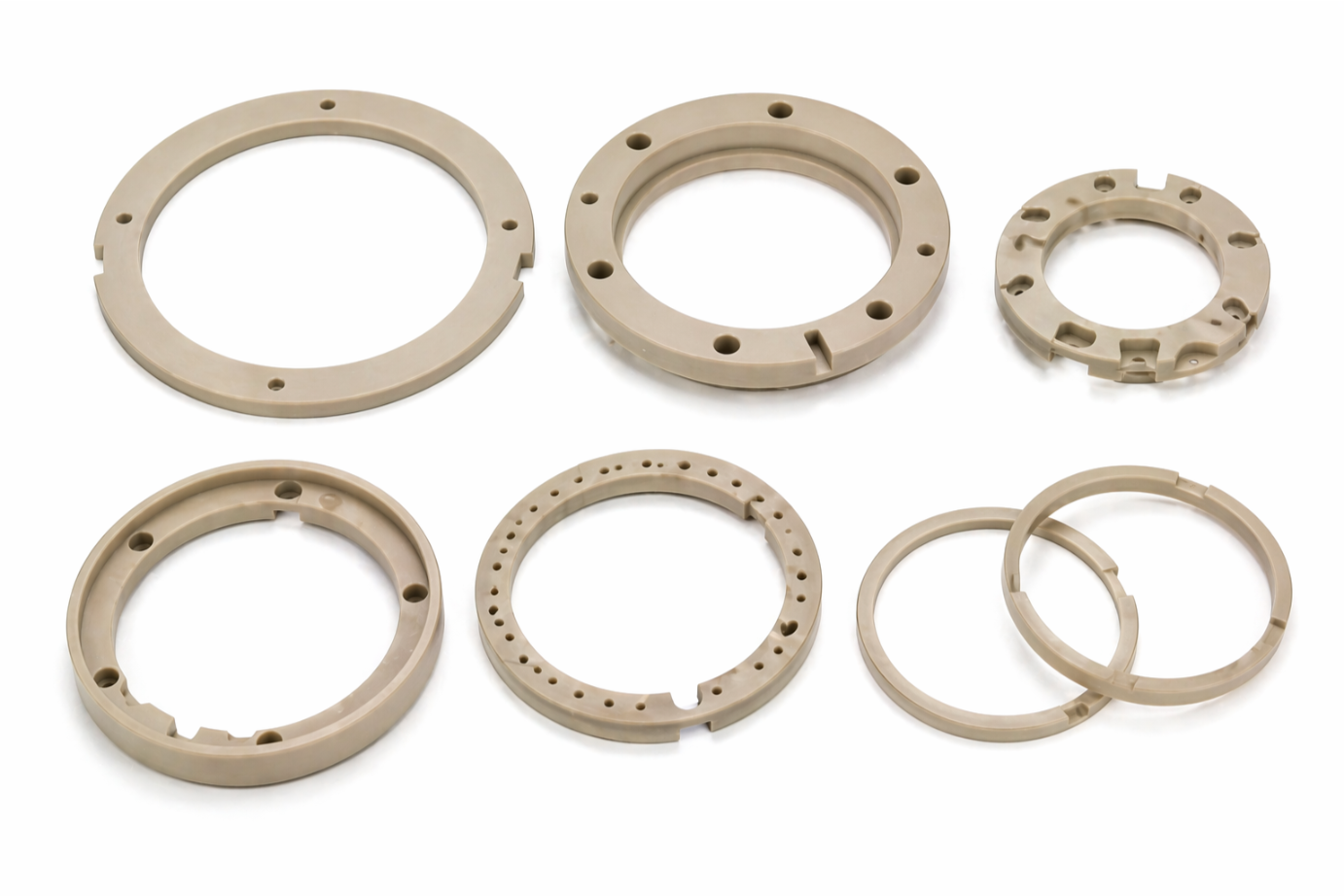
PEEK Wafer Locating Ring
PEEK wafer locating ring for edge contact. ±0.005 mm diameter, Ra 0.4 μm contact surface. Batch of 50 with full dimensional report.

High-Flatness MIC-6 Mounting Plate
MIC-6 cast aluminum mounting plate, lapped to flatness ≤0.01 mm over 400 mm span. Anodize + clean pack. Equipment integration confirmed first attempt.
Common questions from engineers and procurement teams in this industry. Can't find your answer? Ask us directly →