info@hxcnc.com Shenzhen, China Reply within 24 hours
ISO 9001 : 2015 Get Instant Quote
Product Category
≤±0.01mm · ≤50g · Ra 0.4µm · ESD Option
WHG / 001 — 008

Precision CNC
Wafer Handling Grippers

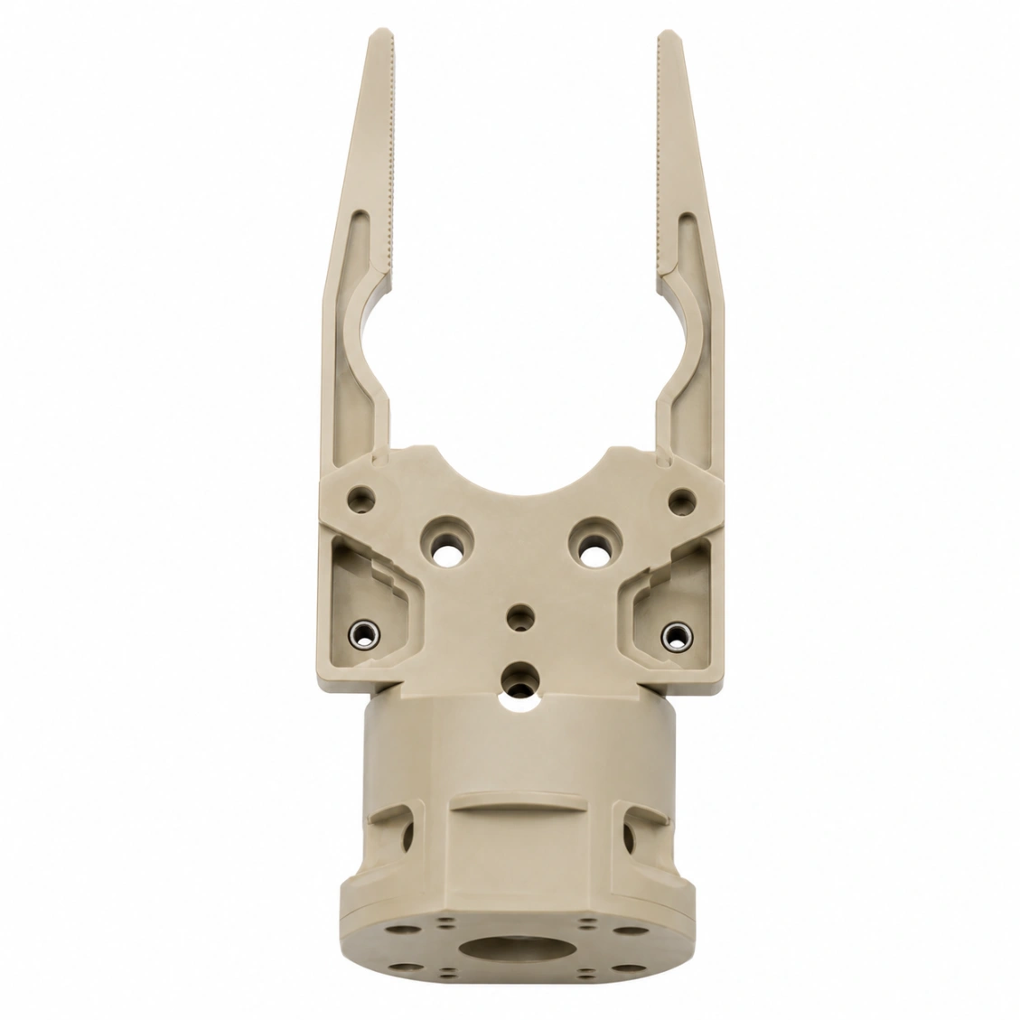
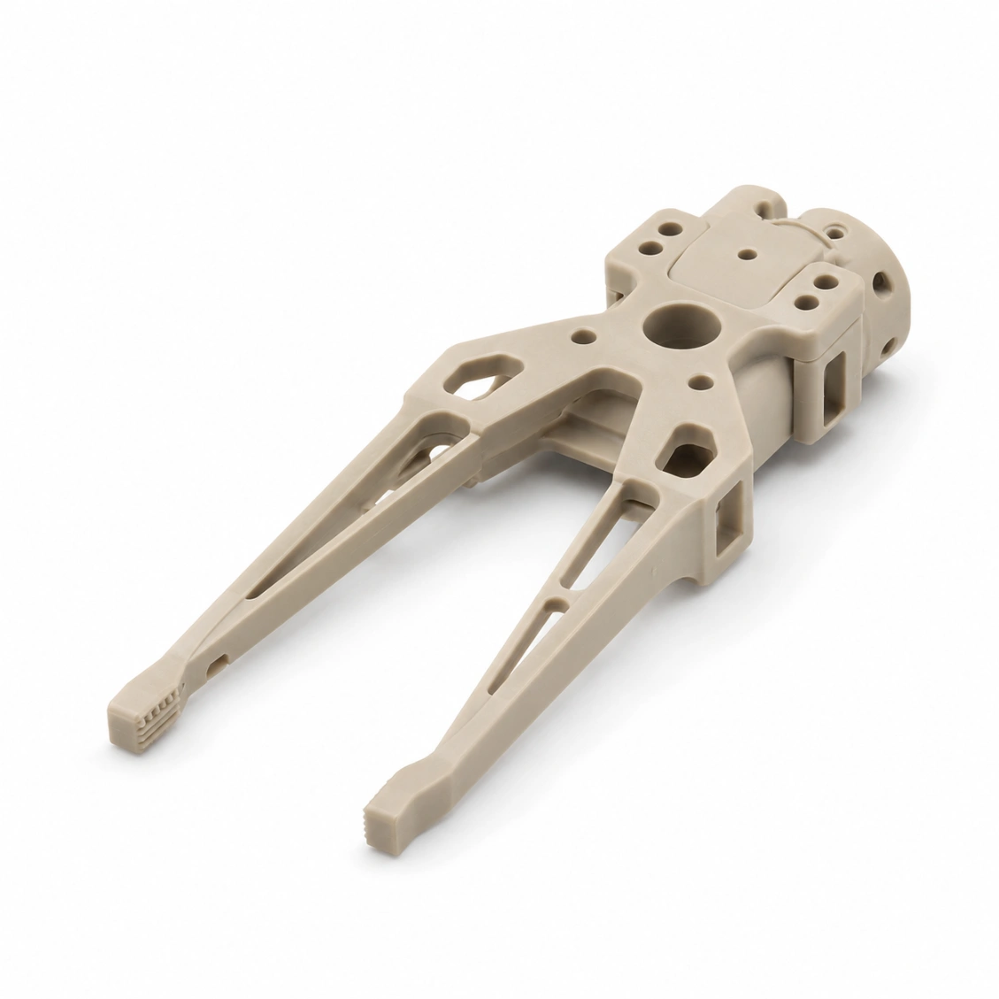
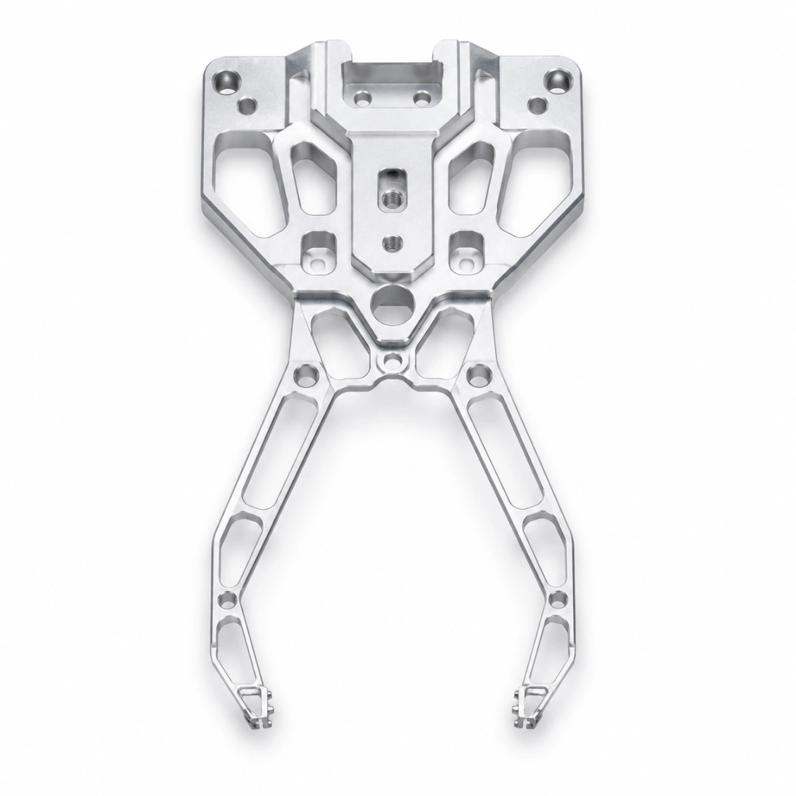
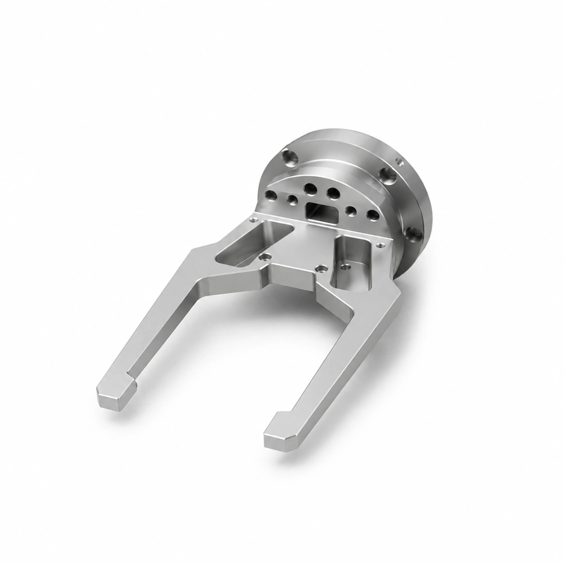
Custom CNC machined wafer handling grippers and end-effectors — contact surface Ra 0.4 µm or better, weight ≤ 50 g for 300 mm wafer grippers, repeat positioning accuracy ≤ ±0.01 mm. Al 7075 anodized or PEEK for cleanroom robot end-effectors.

±0.01mm
Repeat Pos.
≤50g
Weight 300mm
Ra 0.4µm
Contact Surf.
PART DWG · WHG-000 ROBOT END-EFFECTOR · Al 7075 HARD ANODIZE ISO 9001 · ESD COMPATIBLE
Topology Pocketed
3-Pt Vee-Groove
V1 V2 F3 Ø300 WAFER 47 g · −61% vs 120 g SOLID · ≤±0.01 REPEAT WEIGHT · 300mm GRIPPER 120g SOLID 47g ◀ POCKET 35g Ti HOLLOW ↑ inertia ↑ cost VEE-GROOVE · X-SECT 90° DETERMINISTIC edge-only contact ✓ no flat scratch ✓ no Z-drop ✓ repeat ±0.01 ESD · OPTIONS OPTION Ω/sq Cond. anod ◀ 10⁵-10⁸ ESD PEEK 10⁴-10⁶ DLC coat 10⁶-10⁹ Bare Al 7075 conductor Bare PEEK ✗ insulator GRIPPER · MATERIAL MATERIAL DENSITY USE Al 7075 HA ◀ 2.81 standard PEEK 1.31 chemical ESD PEEK 1.42 ESD safe Ti Grade 5 4.43 ultra-light SUS316L 8.00 high-temp SCALE 1 : 2 · MM
FOUP · Robot · Process · Transport
Use Cases
Al 7075 HA · PEEK · ESD PEEK · Ti
Materials
48hr Quote · 6-Day Proto
Service
≤±0.01mm
Repeat Positioning
gripper accuracy
≤50g
Weight Target
300 mm wafer gripper
Ra 0.4µm
Contact Surface
wafer-safe finish
6 Days
Fastest Delivery
prototype orders
Machining Challenges

Wafer Handling Gripper Challenges

A wafer gripper must be simultaneously light (to minimise robot inertia), precise (≤ ±0.01 mm repeat), and damage-proof — the contact surface must never mark a wafer.

⚖️
Weight Minimisation
Every gram of gripper mass adds inertia that the robot motor must overcome — and reduces maximum arm speed or acceleration for a given payload. HXC designs internal pockets and hollow sections into wafer grippers, typically achieving 40–50% weight reduction vs solid while maintaining stiffness.
🔬
Contact Surface Quality
The gripper finger contact points must be polished to Ra 0.4 µm and dimensionally consistent across all fingers — any surface irregularity or height mismatch between contact points causes the wafer to tilt, dropping the wafer or creating stress marks. All contact surfaces are verified by profilometer and CMM.
🔁
Repeat Positioning Accuracy
The gripper must pick and place wafers to ≤ ±0.01 mm repeatably over thousands of cycles. This requires: precise contact geometry (pocket or vee-groove) machined to IT5, and rigidity sufficient to resist spring-back under wafer weight.
Our Work

Wafer Handling Grippers We've Made

Real CNC machined semiconductor components — cleaned, inspected, and cleanroom-packaged.
Request Similar Part
300mm Wafer Gripper Robot End
200mm Wafer End-Effector
PEEK Wafer Gripper Cleanroom
FOUP Gripper Finger
Wafer Transport Gripper
Chemical Process Gripper
Thinned Wafer Gripper
Wafer Grippers Batch
Capabilities & Tolerances

What We Can Deliver

Typical specifications — confirm exact requirements at enquiry.

Repeat positioning≤ ±0.01 mm
Weight (300 mm)≤ 50 g (optimised)
Contact surface Ra0.4 µm or better
Contact geometryVee-groove, pocket, or custom
Wafer sizes100 mm, 150 mm, 200 mm, 300 mm
Material compatibilityCleanroom-certified materials only
MaterialsAl 7075 (hard anodized), PEEK, SUS316L
ESD optionESD PEEK or conductive Al+coating
CleaningIPA ultrasonic + cleanroom pack
Lead time (proto)6–9 days
Lead time (batch)10–16 days
Matched setsAll fingers verified as a set
How It Works

From Drawing to Cleanroom-Ready Part

Upload your drawing — DFM review, machining, cleaning, inspection, and cleanroom packaging within agreed lead time.

01
Upload Drawing
STEP, DXF, PDF. Include material, tolerance, and cleanliness class.
02
DFM & Quote
Free DFM review — sealing face feasibility, thin walls, deburring strategy. Quote in 48 h.
03
Machine, Clean & Inspect
CNC machining, ultrasonic clean, CMM inspection, cleanroom packaging.
04
Ship Worldwide
Full dimensional report + cleaning record enclosed. DHL / FedEx / sea freight.
Reviews

Trusted by Semiconductor Equipment Engineers

★★★★★
"Surface cleanliness and packaging met our cleanroom incoming inspection requirements immediately. Dimensional report matched our CMM check perfectly."
LW
Li Wei
Process Equipment Engineer · Taiwan
★★★★★
"HXC understood the vacuum sealing requirements for our chamber components without lengthy explanation. Lead time was exactly as quoted."
SL
Sophie L.
Equipment Design Engineer · South Korea
★★★★★
"We've sourced wafer handling and chamber parts from HXC for two years. Cleanliness, dimensional accuracy, and batch consistency are excellent."
JT
James T.
Senior Procurement · USA
FAQ

Frequently Asked Questions About Wafer Handling Gripper Machining

Engineering and procurement questions answered by our semiconductor components team.

Contact surfaces are polished to Ra 0.4 µm with no machining marks, burrs, or sharp edges. All contact edges are chamfered and micro-deburred. Material: hard-anodized Al 7075 (HV 400+ surface, no particle shedding) or PEEK (soft, non-scratching). Contact geometry (vee-groove, pocket) is dimensioned to support the wafer at the edge only — not the flat surface.
Standard solid Al 7075 300 mm gripper blank: ~120 g. With HXC's topology-informed pocket milling (removing all non-structural material while retaining stiffness at contact points and arm joints): 45–55 g is achievable. Ti Grade 5 hollow grippers: ~35 g with higher cost.
Contact pocket or vee-groove geometry is machined to IT5 tolerance. All contact positions are measured by CMM as a set — any height or position mismatch between contact points is corrected before the gripper is approved. Stiffness at the wafer contact zone is sufficient to resist deflection under wafer weight (300 mm wafer: ~130 g).
Three-point kinematic contact (two vee-grooves + one flat, or three vee-grooves) provides deterministic wafer location. Vee-groove angle: typically 90°, dimensioned for the wafer edge thickness. For vacuum-chuck grippers: HXC machines precision vacuum ports and O-ring grooves in the contact surface. Custom contact geometry for special wafer geometries (notch, flat, bevels) is standard.
Yes — two options: (1) Conductive Al with ESD coating: standard Al 7075 with a conductive anodize or ESD-specific coating (surface resistivity 10⁵–10⁸ Ω/sq); (2) ESD PEEK: carbon-loaded PEEK with stable ESD resistivity throughout the material. Both are cleanroom-compatible and particle-safe.
All gripper fingers in a set are measured by CMM for: contact surface height (all fingers within ±0.005 mm of each other), contact geometry position (within ±0.01 mm), and weight (matched within ±0.5 g). Fingers are serialised and shipped as a confirmed matched set — not as individual parts.
Yes — HXC machines integrated vacuum chuck ports with internal vacuum routing channels, O-ring sealing grooves at the wafer contact surface, and quick-connect ports for vacuum line attachment. The vacuum chuck face is machined to ≤ ±0.01 mm flatness to ensure uniform seal across the wafer contact zone.
Prototype: 6–9 days. Batch (20–100 pcs): 10–16 days. Matched 3-finger sets: +1 day for final matching inspection.
Get a Quote

Send Your Drawing.
Get a Quote.

Every enquiry includes a DFM review — tolerance feasibility, material confirmation, and process approach confirmed before production starts. MOQ 1 piece.

24hr
Quote Response
MOQ 1
Prototypes OK
ISO
9001:2015
📐
DFM Review on Every Enquiry
Tolerance feasibility, fixturing strategy, and material confirmation. Specific, actionable feedback — not generic pushback.
🎯
First Article Inspection — Standard
FAI report on every new run. Material certs and surface treatment certs included with every shipment.
🔄
Same Process: Prototype to Production
Process plan from your prototype applies to production batches. No re-qualification when you scale.
3 / 4 / 5-Axis CNC + Turning
Complex structural parts, shafts, housings, and transmission components. Metals and engineering plastics.
ISO 9001:2015 3/4/5-Axis Milling CNC Turning CMM Inspection Global Delivery